Summary: Most connected devices don’t fail certification in the test lab. They fail it months earlier, on the first PCB layout, when grounding, antenna position, cables and connector filtering are decided. Here are the five decisions we now make on the first layout, why each one matters for EMC and radio approval, and what has changed since the EU’s radio cybersecurity rules started to apply on 1 August 2025.
Why certification is decided long before the lab
By the time a product reaches the EMC chamber, the board, the enclosure and the antenna are fixed. If emissions are too high or the device resets during an ESD test, every fix is a late one: a board respin, a shield can, a ferrite on a cable or an extra filter that nobody budgeted for. Each of them costs weeks, and some of them cost unit price for the life of the product.
In energy products such as inverters and chargers it’s even harder. The power stage, with fast switching edges and high currents, often sits right next to the radio and the processor.
We’ve been there with our own products: new board revisions and extra components late in the project, more than once. It cost us time and money, and it’s why certification is now part of our first layout review, not a step at the end.
Five decisions to make on the first layout
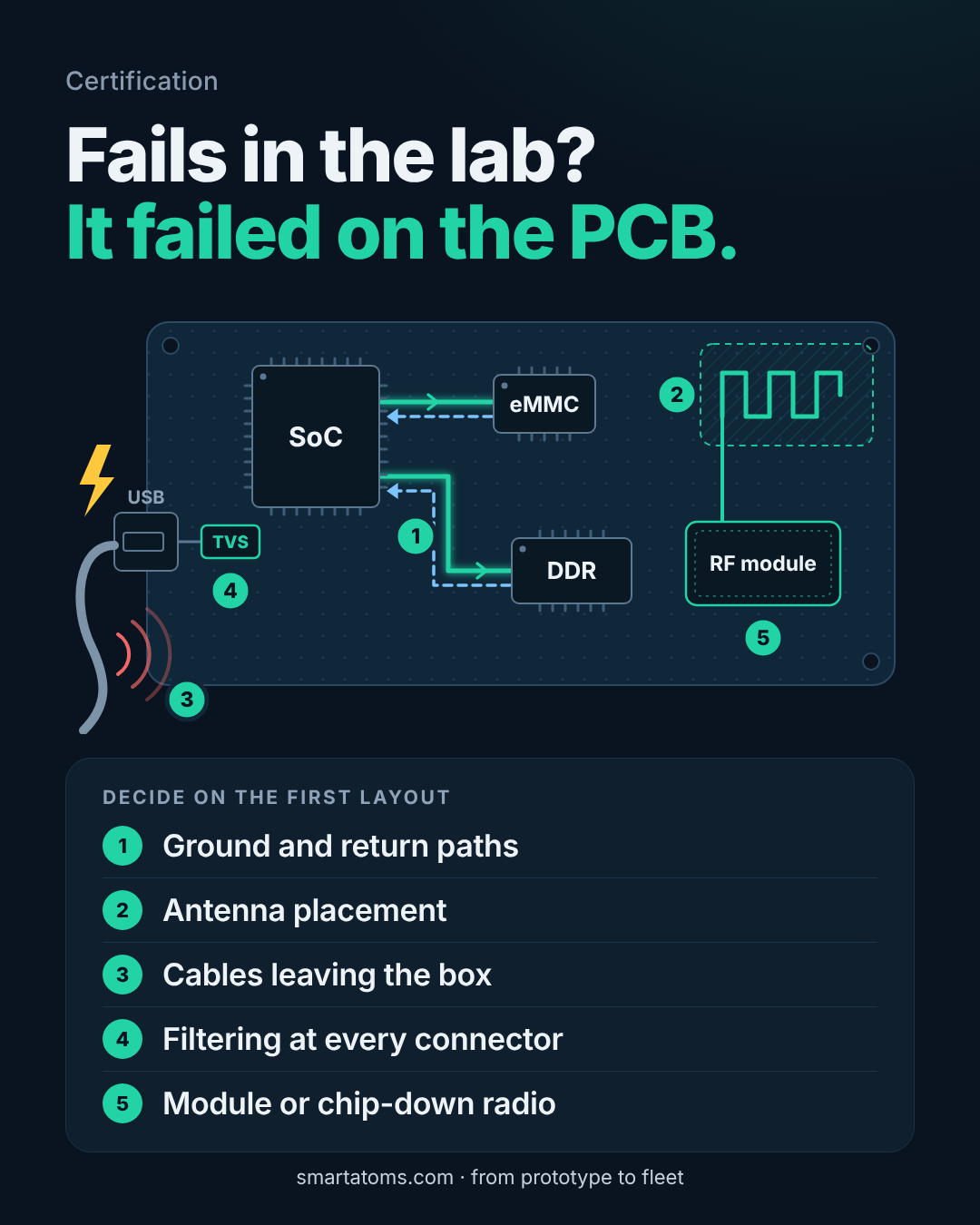
- Ground and return paths for every fast signal. Displays, DDR memory, USB and switching regulators all need a short, unbroken return path. A split ground plane under a fast trace turns it into an antenna. This is the most common root cause of radiated emissions, and the hardest to fix later.
- Where the antenna sits. Decide early what metal, battery, display or power stage will be near the antenna, and keep a clear zone around it. An antenna that works on the evaluation board can lose much of its range inside the final enclosure.
- Which cables leave the enclosure. Every cable that leaves the box is an antenna you didn’t design. Know which signals run on each cable, and plan filtering and shielding where they leave the board.
- Filtering at every connector a user can touch. ESD comes in from outside: USB ports, buttons, connectors and metal parts of the housing. Put protection (for example TVS diodes) and filtering right at the connector, before the signal reaches the rest of the board.
- Pre-certified radio module or chip-down radio. A pre-certified module brings radio test reports with it and gets you to market faster. A chip-down design can lower the unit cost, but the radio part of certification is then yours. Decide this before the layout starts, because it changes the board, the antenna design and the test plan.
Since 1 August 2025: cybersecurity is part of the radio certificate
Radio products sold in the EU now also have to meet the cybersecurity requirements of the Radio Equipment Directive (Delegated Regulation (EU) 2022/30), with the harmonised standards EN 18031-1, -2 and -3. In practice this covers network protection, personal data and, for some products, payments: no universal default passwords, secure update mechanisms, protection of stored and transmitted data.
That means firmware and update design are no longer only a software topic. They are part of what a radio product needs to be placed on the EU market, and the EU Cyber Resilience Act will add further requirements for products with digital elements.

A rule of thumb: pre-scan the first prototype
Run an EMC pre-scan on the first working prototype, not on the production sample. A pre-scan is a quick, informal measurement in a test lab or with near-field probes on your own bench. It won’t certify anything, but it shows where the board radiates and how much margin you have.
A failed pre-scan is cheap: you change the layout of the next revision. A failed certification is a new board, a new round of tests and a later launch.
Checklist before you freeze the layout
- Every fast signal has a continuous return path; no splits in the ground plane under it.
- Antenna keep-out zone defined, and checked against the enclosure, battery and display.
- List of all cables leaving the enclosure, with filtering planned for each.
- ESD protection and filtering at every user-accessible connector.
- Module or chip-down radio decided, with its effect on the test plan.
- Default passwords, update mechanism and data protection planned for the RED cybersecurity requirements.
- Pre-scan booked for the first working prototype.
How we help
We design electronics with certification in mind from the first schematic, and we support the CE, RED and FCC process through to the test reports. See our electronics and PCB design and CE, RED and FCC certification services. If your product is heading for its first EMC test, talk to an engineer.